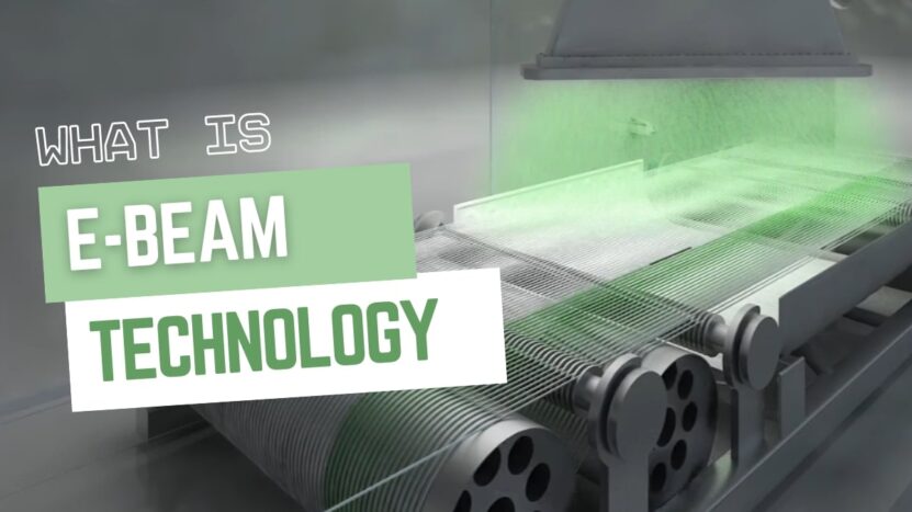
Are you curious about the latest technology trends in the world of electronics and manufacturing? E-beam technology is an exciting development that you should know about. In this article, we will explore everything you need to know about it, including its definition, how it works, its applications, and much more.
The Definition of E-beam Technology
E-beam technology is a process that uses a beam of high-energy electrons to create, manipulate, and analyze materials. This technology is widely used in the manufacturing of semiconductors, biomedical research, and material science. The high-energy electrons in the beam are capable of penetrating solid materials, allowing them to be used for imaging, welding, and lithography.
How Does It Work?
E-beam technology works by producing a beam of high-energy electrons that are then directed toward a sample. When the electrons hit the sample, they can either penetrate the sample or bounce off the surface. The electrons that penetrate the sample can be used to create an image, weld materials, or alter the surface properties of the material.
Types of E-beam Technology
There are several different types of e-beam technology, including Scanning Electron Microscope (SEM), Transmission Electron Microscope (TEM), Electron Beam Lithography (EBL), and Electron Beam Welding (EBW). In this section, we are going to explain each of them.
1. Scanning Electron Microscope (SEM)
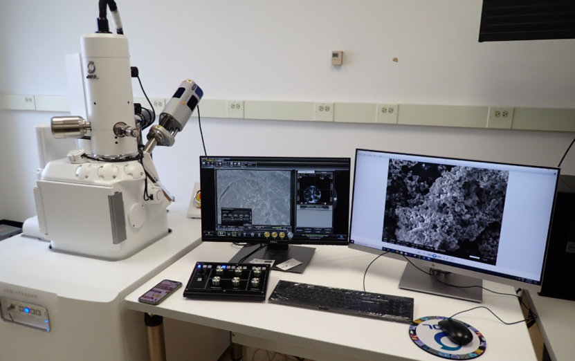
SEM works by scanning a beam of high-energy electrons over the surface of the material, revealing a 3D image with stunning clarity. It’s like having a superpower that lets us see the tiniest features and imperfections of any material we want to explore.
It is widely used in research and development, and it’s an essential tool for studying everything from nanomaterials to insects’ eyes.
2. Transmission Electron Microscope (TEM)
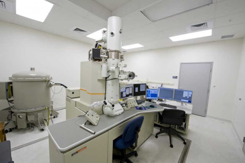
TEM allows us to see through materials and analyze their inner workings. It works by shooting a beam of high-energy electrons through the material, producing an image on the other side. It’s like having a magic microscope that can see the tiniest details of the material’s structure, allowing us to explore the fascinating world of materials science.
It is widely used in research and development, and it’s a critical tool for studying everything from biological samples to semiconductors.
3. Electron Beam Lithography (EBL)
This type is like a magic wand for creating intricate patterns on materials. It works by using a focused beam of electrons to etch out designs and shapes with absolute precision. It’s like painting a masterpiece, but instead of using a brush, you’re using a high-energy electron beam to create your work of art.
EBL is perfect for creating patterns on a variety of materials, from silicon to polymers, and it’s widely used in the manufacturing of microelectronics and other high-tech applications. So, if you want to add some flair to your materials, grab your electron beam wand and start creating!
4. Electron Beam Welding (EBW)
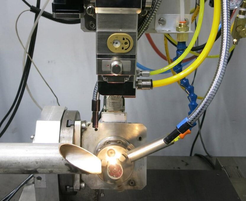
This is the ultimate welding superhero of e-beam technology. It saves the day by using a focused beam of high-energy electrons to melt the material, forming a solid bond that holds materials together with superhero strength. Whether you need to join metals or ceramics, EBW can handle it all with precision and speed.
Applications of E-beam Technology
This technology has a wide range of applications, including:
Manufacturing of semiconductors
E-beam technology is used in the manufacturing of semiconductors, which are used in various electronic devices such as computers, mobile phones, and televisions. E-beam lithography is used to create patterns on the surface of semiconductors, which are then used to create electronic circuits.
Biomedical research
It is also used in biomedical research to study the structure of cells and tissues. TEM is used to produce images of cells and tissues at high magnification, allowing researchers to study their structure in detail.
Material science
SEM and TEM are used to produce images of materials at high magnification, allowing researchers to study their structure in detail. E-beam lithography is also used to create patterns on materials for use in various applications.
Microelectronics
This technology also finds its uses in the production of microelectronics, such as microchips and circuit boards. E-beam lithography is used to create patterns on the surface of the microelectronics, which are then used to create electronic circuits.
Advantages and Disadvantages of E-beam Technology
Like any technology, this one has both advantages and disadvantages. Some of the advantages of e-beam technology include:
- High resolution: It can produce images and patterns at very high resolution, allowing for detailed analysis and manipulation of materials.
- Precise control: It allows for precise control over the beam of electrons, making it possible to create very precise patterns and welds.
- Non-contact: E-beam technology does not require physical contact with the material, which can be useful for delicate materials or materials that are easily damaged.
Some of the disadvantages of e-beam technology include:
- Cost: This technology can be expensive to implement and maintain, making it less accessible for smaller businesses or research institutions.
- Limited depth of penetration: The high-energy electrons in the beam can only penetrate a certain depth into the material, which can limit the usefulness of e-beam technology for certain applications.
- Radiation hazard: E-beam technology can produce radiation, which can be hazardous to human health if not properly controlled.
Future Prospects of E-beam Technology
E-beam technology is a rapidly developing field with many potential applications. Some of the areas where this technology is expected to have an impact in the future include:
Nanotechnology: It has the potential to be used in the production of nanoscale materials and devices.
3D printing: This technology could be used to create precise 3D printed objects with high resolution and accuracy.
Quantum computing: It could be used in the production of quantum computing components, which require extremely precise patterning and manipulation of materials.
Frequently Asked Questions

1. Is e-beam technology safe to use?
Yes, e-beam technology is generally safe to use when proper safety protocols are followed.
2. How is e-beam technology used in the manufacturing of semiconductors?
E-beam lithography is used to create patterns on the surface of semiconductors, which are then used to create electronic circuits.
3. Can this technology be used to weld any material?
No, it is most effective for welding materials with high melting points, such as metals and ceramics.
4. How is e-beam technology used in material science?
E-beam technology is used to produce high-resolution images of materials, allowing researchers to study their structure and properties in detail.
5. Is e-beam technology expensive to implement?
Yes, e-beam technology can be expensive to implement and maintain, making it less accessible for smaller businesses or research institutions.
Final Words
E-beam technology is a fascinating field with many potential applications in electronics, manufacturing, and research. With its high resolution and precise control, e-beam technology has the potential to revolutionize many industries in the future.